CAEN V792
说明书 V792
- Inputs: 32/16 channels, 50 Ω impedance, negative polarity, DC coupling
- Input range: 0 ÷ 400 pC
- Resolution: 12 bit
- Gain: 100 fC/count
- Reflections: <5% with 2 ns fall time input signals
- Noise
- GateWidth(ns) Iped(count) Average(count) σ(count)
- 100 180 107.58 0.50
- 500 180 326.44 0.54
- 1000 180 597.32 0.56
- 2000 180 1139.92 0.61
- Fast clear time: 600 ns
- Gate timing: The GATE signal must precede the analog input by >15 ns
- Conversion time: Mod. V792: 5.7 μs/32 Ch.; Mod. V792 N: 2.8 μs/16 Ch.
- Dead time: Mod. V792: 6.9 μs/32 Ch.; Mod. V792 N: 4 μs/16 Ch.
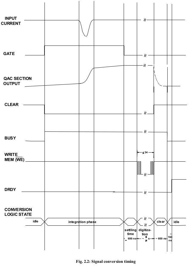
The Model V792 is a 1-unit wide VME 6U module housing 32 Charge-to-Digital Conversion channels with current integrating negative inputs (50 Ω impedance). For each channel, the input charge is converted to a voltage level by a QAC (Charge to Amplitude Conversion) section. Input range is 0 ÷ 400 pC.
The boards are available both for standard and V430 VME crates; all versions support live insertion, allowing the User to insert (or remove) the board into (or from) the crate without switching it off.
A 16 ch. decoupling board (Mod. A992) is available for the Mod. V792 to avoid ground loops and signal reflections when long flat cable (110 Ω) connections to the 50 Ω inputs are used (one 32 ch. V792 requires two A992 boards).
The board has 32 (16 for the Mod. V792 N) input channels and one GATE input(ECL/NIM) common to all channels. The Mod. V792 N does not feature the ECL GATE input.
The integrated currents, received from the channel inputs when the GATE input signal is active, are converted into voltage levels by the QAC sections and then multiplexed and converted by two fast 12-bit ADC modules.
The Mod. V792 inputs can be tested with a voltage generator: in this case it is necessary to put a resitor (~1 kohm) in series to the generator; the integrated charge will be then $Q = [V{GEN}/(1K+50)]*T{GATE}$
Pedestal
The QDC pedestal is the value readout when no input signal is present (open inputs). It is mainly due to the $I{P}$ current integrated by the capacitor C when a GATE signal is applied. It is worth noting that the QDC pedestal does not depend linearly on GATE width. When the maximum dynamic range is needed, it is possible to program $I{1}$ so that $I_{P}$ is close to zero.
Table 2.1 shows that, below 55 DAC counts, the channel is “decoupled” and provides no output.
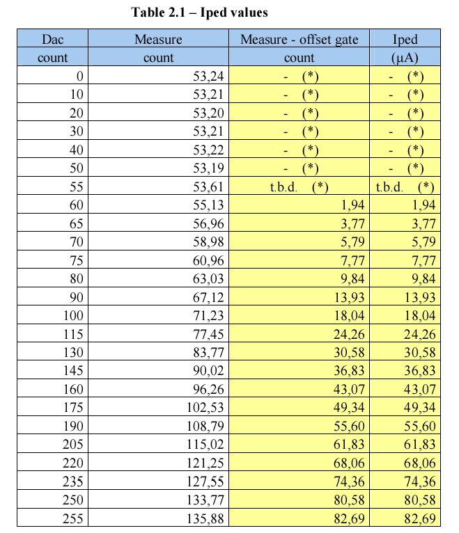
Our advice is not to set the Iped Register below 60 counts in order to guarantee the channels to be “coupled”; anyway if the User wishes to have the channels “coupled” precisely with the minimum possible Iped, then it is necessary to set the Iped Register between 50 and 60 DAC counts and to increase the gate in order to check that the readout counts grows as the gate grows; if this does not happen, then Iped Register must be increased.
Maximum GATE width
The pedestal current value $I{P}$ sets an upper limit on the maximum GATE width. The QDC pedestal value is ${TGATE}* I{P}$ ,where TGATE is the GATE width; usually, in order not to spoil the QDC dynamic range, this pedestal value should be 5-10% of the FSR. For example, if $I{P}$ ∼1 μA and at least 90% of the dynamic range is needed, the GATE width should not exceed ∼ 40 μs.
FAST CLEAR
The FAST CLEAR of the module can be performed via the relevant front panel signal. A FAST CLEAR signal, generated at any time within the FAST CLEAR window, i.e. between the leading edge of the GATE signal and the end of the programmable time value set in the Fast Clear Window Register, aborts the conversion. Its minimum width must be 30 ns.
N.B.: since a FAST CLEAR operation implies a CLEAR CONVERSION cycle, a new GATE signal is accepted only if it occurs at least 600 ns after the leading-edge of the FAST CLEAR signal.